

General Specification
| Item | Nominal Dimension | Unit |
|---|---|---|
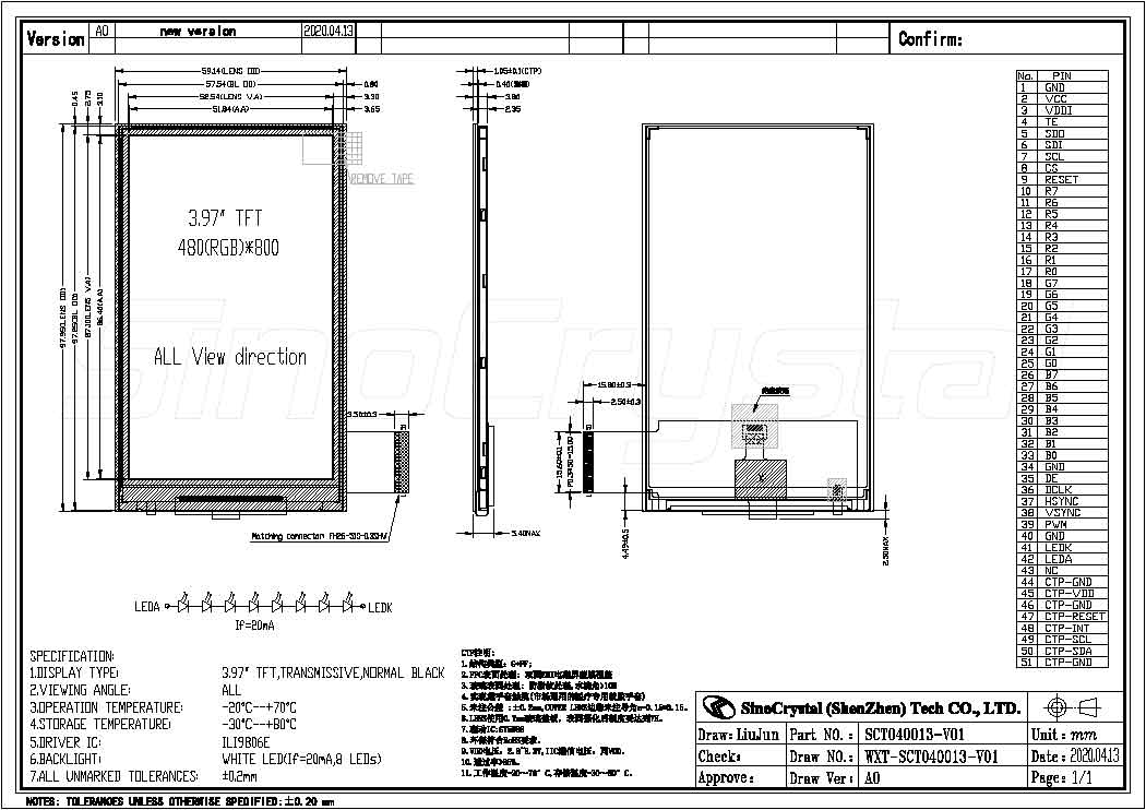
| Dot Matrix | 480 x RGB x 800 | Dots |
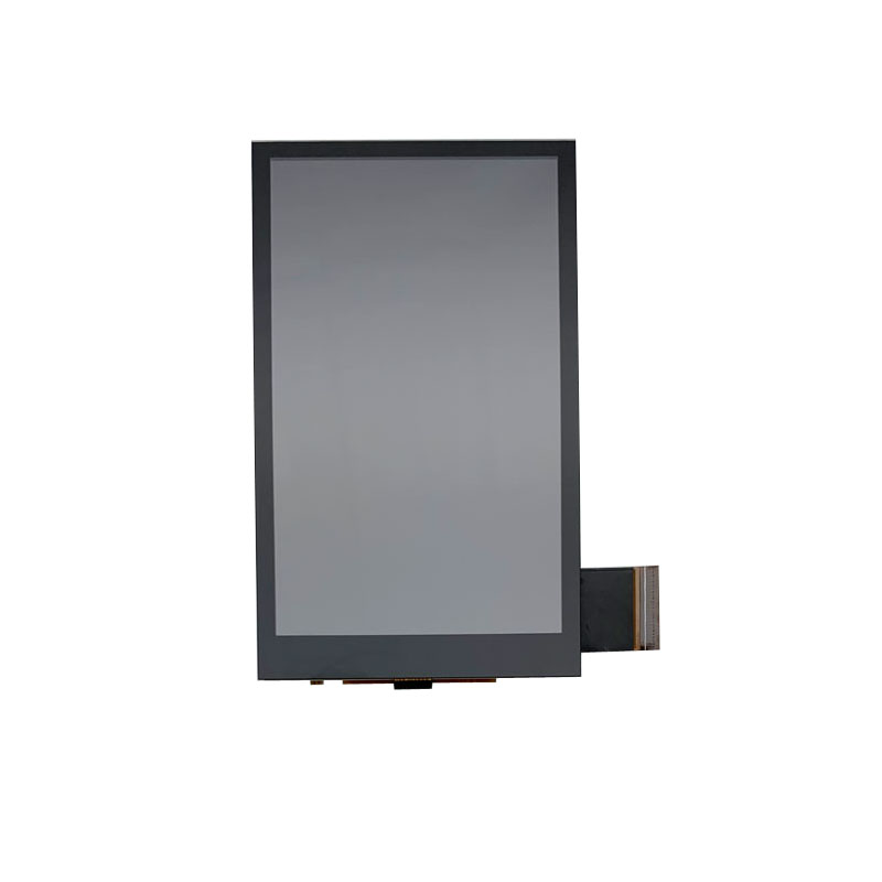
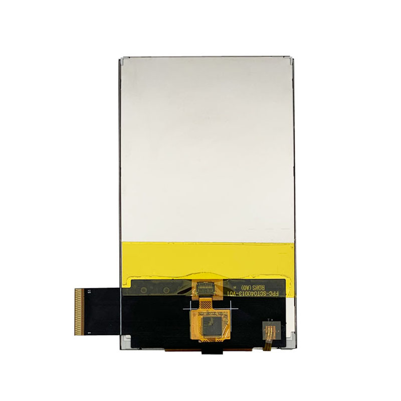
| Module Size ( W×H×T ) | 59.14 × 97.95 × 3.80 | mm. |
| Active Area ( W×H ) | 51.84 × 86.40 | mm. |
| Pixel arrangement | R.G.B. Stripe | mm. |
| Dot Pitch ( W×H ) | 0.108 × 0.108 | mm. |
| Color depth | 16.7M | colors |
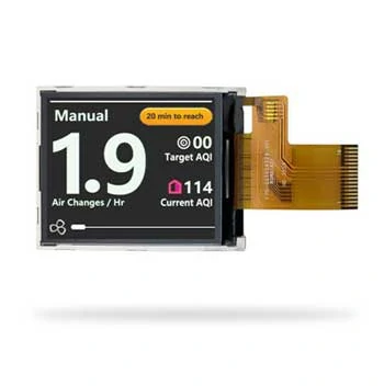
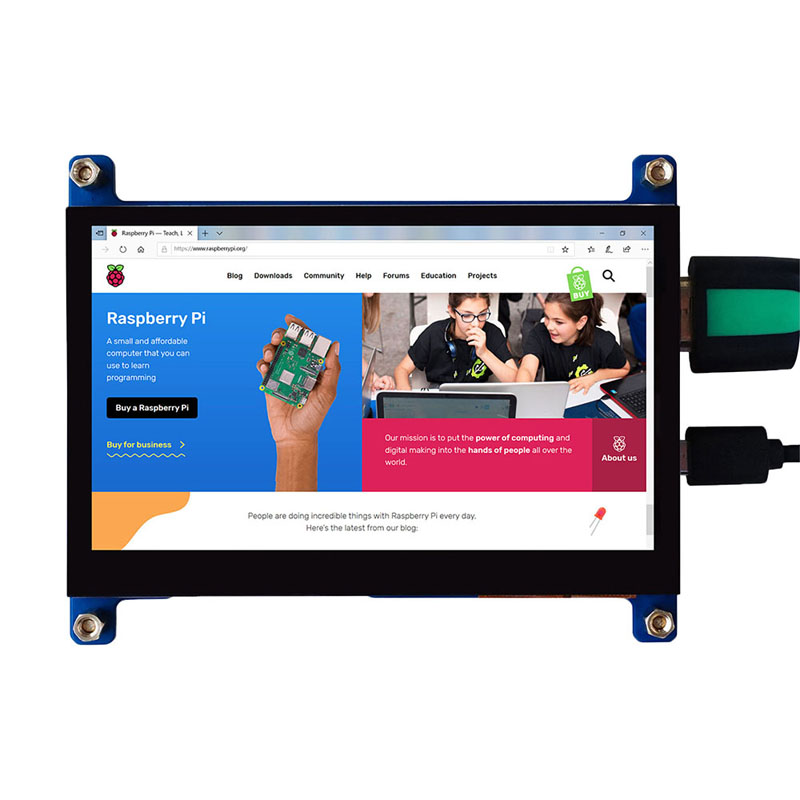
| Interface | SPI + RGB | – |
| Display Mode | Normally Black, Transmissive | – |
| Operating temperature | -20 ~70 | ºC |
| Storage temperature | -30~80 | ºC |
| LCD Type | IPS | – |
| LCD Mode | Normal Black | – |
| Backlight Type | LED x 8 | PCS |
Interface Definition
| Pin No. | Symbol | Type | Description |
|---|---|---|---|
| 1 | GND | P | Ground |
| 2 | VCC | P | Power supply for system |
| 3 | VDDI | P | Power supply for I/O |
| 4 | TE | O | Tearing effect output |
| 5 | SDO | O | Serial data output |
| 6 | SDI | I | Serial data input |
| 7 | SCL | I | Serial interface clock |
| 8 | CS | I | Chip Select signal |
| 9 | RESET | I | Chip reset signal |
| 10-17 | R7 – R0 | I | Data bus for Red |
| 18-25 | G7 – G0 | I | Data bus for Green |
| 26-33 | B7 – B0 | I | Data bus for Blue |
| 34 | GND | P | Ground |
| 35 | DE | I | Data enable input |
| 36 | PCLK | I | Pixel clock input |
| 37 | HSYNC | I | Horizontal sync input |
| 38 | VSYNC | I | Vertical sync input |
| 39 | PWM | O | PWM frequency output for LED driver control (open when not in use) |
| 40 | GND | P | Ground |
| 41 | LEDK | P | LED driving cathode |
| 42 | LEDA | P | LED driving anode |
| 43 | NC | – | No connection |
| 44 | CTP-GND | P | Ground for CTP |
| 45 | CTP-VDD | P | Power supply for C |